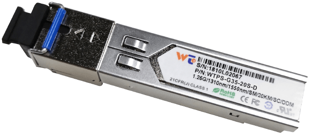
WTPS-G35–20S-D/ WTPS-G53–20S-D
1.25Gbps BIDI SFP Optical Transceiver 20Km DDM
- Feature:
- SFP package with SC connector
- 1310nm FP Laser and 1550nm PIN photodetector
- 1550nm DFB Laser and 1310nm PIN photodetector
- Up to 20Km transmission on SMF
- +3.3V single power supply
- LVPECL compatible data input/output interface
- Low EMI and excellent ESD protection
- laser safety standard IEC-60825 compliant
- Compatible with RoHS
- Compatible with SFF8472
- Application:
- 25Gb/s 1000Base-LX Ethernet
- 06 Gb/s Fibre ChannelFiber Channel
- Absolute Maximum Ratings:
Parameter Symbol Minimum Maximum Units Storage Temperature Tst -40 +85 °C Supply Voltage Vcc 0 +3.6 V Operating Relative Humidity RH 5 95 %
- Operation Environment:
Parameter Symbol Min Typical Max Units Supply Voltage Vcc 3.15 3.3 3.45 V Operating Case Temperature TC 0 +70 ℃ Power Dissipation 1 W Data Rate 1.25 Gbps
5.OpticalCharacteristics:
(Ambient Operating Temperature 0°C to +70°C, Vcc =3.3 V)
| Parameter | Symbol | Min. | Typ. | Max. | Units | |
| Transmitter Section | ||||||
| Center Wavelength | Tx1310 | lo | 1260 | 1310 | 1360 | nm |
| Tx1550 | 1540 | 1550 | 1560 | |||
| Spectral Width(RMS) | Tx1310 | Dl | – | – | 4 | nm |
| Tx1550 | 1 | |||||
| Average Output Power | Tx1310 | Po | -9 | – | -3 | dBm |
| Tx1550 | -9 | -3 | ||||
| Extinction Ratio | Er | 8 | – | dB | ||
| Rise/Fall Time(20%~80%) | Tr/Tf | 300 | ps | |||
| Total jitter | Tj | 0.43 | UI | |||
| Optical Eye Diagram | IEEE 802.3z and ANSI Fibre Channel Compatible | |||||
| Receiver Section | ||||||
| Center Wavelength | Rx1550 | lo | 1500 | 1550 | 1600 | nm |
| Rx1310 | 1260 | 1310 | 1360 | |||
| Receiver Sensitivity | Rsen | -22 | dBm | |||
| Receiver Overload | Rov | -3 | dBm | |||
| Return Loss | 12 | dB | ||||
| LOS Assert | LOSA | -36 | dBm | |||
| LOS Dessert | LOSD | -23 | dBm | |||
| LOS Hysteresis | 0.5 | 5 | ||||
- Electrical Characteristics:
(Ambient Operating Temperature 0°C to +70°C, Vcc =3.3 V)
| Parameter | Symbol | Min. | Typ. | Max. | unit | |
| Transmitter Section | ||||||
| Input Differential Impendence
|
Zin | 90 | 100 | 110 | Ohm | |
| Data Input Swing Differential | Vin | 500 | 2400 | mV | ||
| TX Disable | Disable | 2.0 | Vcc | V | ||
| Enable | 0 | 0.8 | V | |||
| TX Fault | Assert | 2.0 | Vcc | V | ||
| Deassert | 0 | 0.8 | V | |||
| Receiver Section | ||||||
| Output differential impendence | Zout | 100 | Ohm | |||
| Data Input Swing Differential | Vout | 370 | 2000 | mV | ||
| Rx_LOS | Assert | 2.0 | Vcc | V | ||
| Deassert | 0 | 0.8 | V | |||
- EEPROM INFORMATION(A0):
Addr Field Size (Bytes)
Name of Field HEX Description 0 1 Identifier 03 SFP 1 1 Ext. Identifier 04 MOD4 2 1 Connector 01 SC 3-10 8 Transceiver 00 00 00 02 12 00 0D 01 Transmitter Code 11 1 Encoding 01 8B10B 12 1 BR, nominal 0D 1250M bps 13 1 Reserved 00 14 1 Length (9um)-km 14 20km 15 1 Length (9um) 64/C8/FF 16 1 Length (50um) 00 17 1 Length (62.5um) 00 18 1 Length (copper) 00 19 1 Reserved 00 20-35 16 Vendor name 57 49 4E 54 4F 50 20 20 20 20 20 20 20 20 20 20
WINTOP 36 1 Reserved 00 37-39 3 Vendor OUI 00 00 00 40-55 16 Vendor PN xx xx xx xx xx xx xx xx xx xx xx xx xx xx xx xx
ASC II 56-59 4 Vendor rev 31 2E 30 20 V1.0 60-61 2 Wavelength 05 1E/05 D2 1310nm/1550nm 62 1 Reserved 00 63 1 CC BASE XX Check sum of byte 0~62 64-65 2 Options 00 1A LOS, TX_DISABLE, TX_FAULT 66 1 BR, max 32 50% 67 1 BR, min 32 50% 68-83 16 Vendor SN 00 00 00 00 00 00 00 00 00 00 00 00 00 00 00 00
Unspecified 84-91 8 Vendor date code XX XX XX 20 Year, Month, Day 92-94 3 Reserved 00 95 1 CC_EXT XX Check sum of byte 64~94 96-255 160 Vendor specific
- Diagnostics:
Parameter Range Accuracy Unit Calibration Temperature 0 ~ 70 ±5 ºC Internal Voltage 3-15 ~ 3.45 0.1 V Internal Bias Current 10 ~ 80 ±2 mA Internal Tx Power -9 ~ -3 ±2 dBm Internal Rx Power -26~-3 ±3 dBm Internal
- Pin Description:
Pins Name Discription NOTE 1 VeeT Transmitter Ground 2 Tx Fault Transmitter Fault Indication 1 3 Tx Disable Transmitter Disable 2 4 MOD DEF2 Module Definition 2 3 5 MOD DEF1 Module Definition 1 3 6 MOD DEF0 Module Definition 0 3 7 Rate Select Not Connected 8 LOS Loss of Signal 4 9 VeeR Receiver Ground 10 VeeR Receiver Ground 11 VeeR Receiver Ground 12 RD- Inv. Received Data Output 5 13 RD+ IReceived Data Output 5 14 VeeR Receiver Ground 15 VccR Receiver Power 16 VccT Transmitter Power 17 VeeT Transmitter Ground 18 TD+ Transmit Data Input 6 19 TD- Inv. Transmit Data Input 6 20 VeeT Transmitter Ground
Notes:
- TX Fault is an open collector output, which should be pulled up with a 4.7k~10kΩ resistor on the host board to a voltage between 2.0V and Vcc+0.3V. Logic 0 indicates normal operation; logic 1 indicates a laser fault of some kind. In the low state, the output will be pulled to less than 0.8V.
- TX Disable is an input that is used to shut down the transmitter optical output. It is pulled up within the module with a 4.7k~10kΩ resistor. Its states are:
Low (0~0.8V): Transmitter on
(>0.8V, <2.0V): Undefined
High (2.0~3.3V): Transmitter Disabled
Open: Transmitter Disabled
- MOD-DEF 0,1,2 are the module definition pins. They should be pulled up with a 4.7k~10kΩ resistor on
the host board. The pull-up voltage shall be VccT or VccR.
MOD-DEF 0 is grounded by the module to indicate that the module is present
MOD-DEF 1 is the clock line of two wire serial interface for serial ID
MOD-DEF 2 is the data line of two wire serial interface for serial ID
- LOS is an open collector output, which should be pulled up with a 4.7k~10kΩ resistor on the host board to a voltage between 2.0V and Vcc+0.3V. Logic 0 indicates normal operation; logic 1 indicates loss of signal. In the low state, the output will be pulled to less than 0.8V.
- These are the differential receiver output. They are internally AC-coupled 100Ω differential lines which should be terminated with 100Ω (differential) at the user SERDES.
- These are the differential transmitter inputs. They are AC-coupled, differential lines with 100Ω differential termination inside the module.
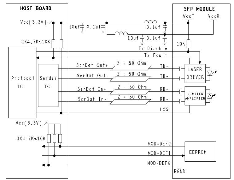
- Recommended Application Circuit:

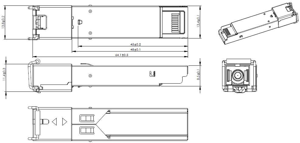
- Outline Dimensions (mm):